
Understanding copper interconnects, optical engines, CPO, OCS and fiber arrays
When one chip sends data to another, the information travels through a physical medium. Copper interconnects carry electrical signals; optical fibers carry light. Understanding where conversion takes place helps explain why both technologies remain important in high-speed systems.
A common misconception is that reaching a 224G electrical lane rate means every connection must become optical. In practice, short copper links can remain attractive when they meet the channel requirements. Optical links become more compelling as reach, density and energy constraints increase.
The decision depends on the complete system: signaling format, channel loss, cable construction, connectors, equalization, thermal limits and serviceability. This article separates the underlying physics from implementation choices and explains how the main components fit together.
1.Copper interconnects and the limits of reach
What an electrical signal actually does
Electrical data is conveyed by changing voltage and current, with electromagnetic energy propagating along the transmission structure. Individual electrons do not travel from one chip to the other at the signal propagation speed. Copper offers mature manufacturing, familiar connectors and, in passive links, no optical conversion or cable-side active electronics. These advantages make it a strong option for many short connections.
Three challenges at higher signaling frequencies
Skin effect. At high frequencies, current becomes concentrated near a conductor’s surface, increasing its effective AC resistance. In a simplified skin-effect model, conductor loss rises approximately with the square root of frequency. Surface roughness and real geometry introduce additional effects; the loss should not be described as universally exponential with data rate.
Dielectric loss. Insulating materials around conductors and in PCB laminates dissipate some signal energy as heat. Over a useful frequency range, dielectric attenuation often increases approximately with frequency when material properties remain similar. Material selection, trace geometry and total channel length all matter.
Crosstalk and impedance discontinuities. Adjacent channels can couple energy into one another, while connectors, vias and geometry changes can create reflections. Differential-pair imbalance adds further impairments. Together, these effects reduce the receiver’s ability to distinguish signal levels reliably.
Equalization compensates for some channel distortion. Retimers can recover and regenerate signals between channel segments, extending useful system reach at the cost of power, latency and complexity. They do not eliminate the physical losses of each segment.
224G and 448G do not have one universal distance limit
Board traces, backplanes and cable assemblies are different channel types. A passive direct-attach copper cable, or DAC, should also be distinguished from an active electrical cable containing signal-conditioning electronics. A retimed cable is not a passive DAC.
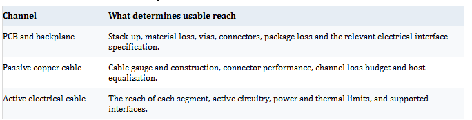
224G-class signaling can support short electrical interconnects, but a distance such as one or two meters must be tied to an actual qualified design. Likewise, 0.5 m is not a universal boundary for 448G. OIF’s CEI-448G framework explores channel objectives and modulation alternatives, including PAM4, PAM6 and PAM8; a demonstration is not proof of widespread deployment.
2.Why optical links extend the useful reach
Optical fibers guide light in their cores. They avoid the conductor skin effect and electrical crosstalk mechanisms that constrain copper channels, making them well suited to longer links and high aggregate bandwidth.
Fiber is low loss, not lossless. Attenuation, connectors, splices, bends and fiber-to-chip coupling consume optical power. Dispersion and other impairments can also limit performance. A practical link must meet a defined optical power and signal-quality budget. Very long links require optics designed for that reach; they are not simply longer versions of a short data center connection.
A fiber infrastructure may support successive bandwidth generations, but an upgrade from 800G to 1.6T or 3.2T does not automatically preserve every component. Fiber type, wavelength plan, lane count, connectors and transceiver requirements must remain compatible.
3.How optical engines convert signals
An optical engine provides the conversion functions between electronic circuitry and an optical link. Implementations integrate these functions in different ways; the diagram shows the basic signal flow rather than a particular product design.
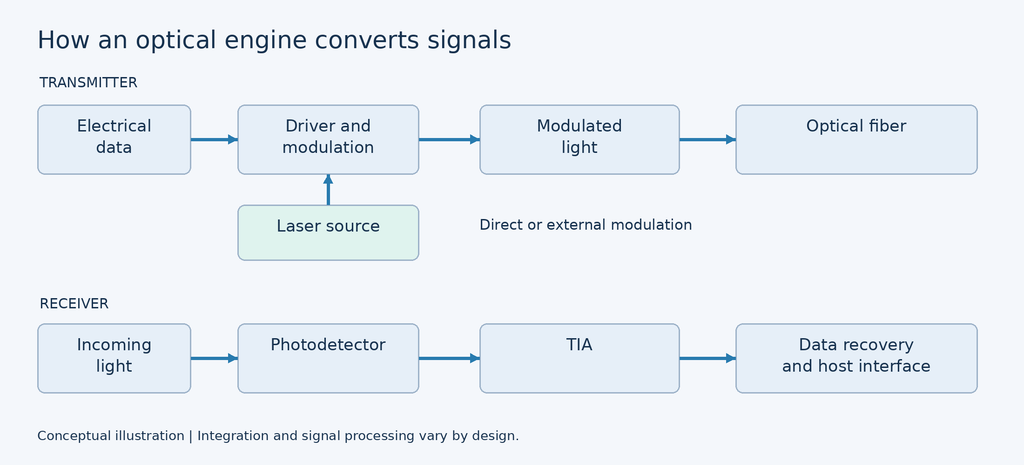
Transmitter electrical data becomes modulated light
A driver supplies the electrical swing and waveform required by the optical transmitter. A laser provides light, and modulation places the data onto that light. Some designs modulate the laser directly; others use a separate modulator. DFB lasers, EMLs, VCSELs and external laser sources represent different architectures rather than interchangeable parts of one universal arrangement.
Intensity modulation is common in short-reach links. Coherent systems can also encode information in optical phase and other dimensions. The transmitter design determines which approach is used.
Receiver light becomes electrical data
A photodetector converts received optical power into current. A transimpedance amplifier, or TIA, converts that current into a voltage signal. Subsequent circuitry processes the signal and recovers data; clock recovery, equalization, DSP and error correction depend on the link architecture. A receiver does not remove all noise, and photocurrent is not always at a fixed nanoampere level.
For practical examples of electrical-to-optical conversion in AV and peripheral connectivity, explore Elike’s optical modules for HDMI, DisplayPort and USB.
4.Optical engines and optical modules
An optical engine is the conversion core. An optical transceiver module packages optical and electronic functions into a usable subsystem, often adding a standardized electrical interface, management functions, power circuitry, mechanical protection and thermal provisions. A pluggable module is one implementation; optical engines also appear in more integrated assemblies.
The shift toward closer integration aims to shorten the high-speed electrical path between the host ASIC and the optical conversion point. The main approaches differ in where the optics sit and how they can be assembled, cooled and serviced.
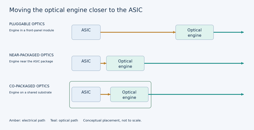
Pluggable optics
The optical engine sits inside a module at the equipment front panel. This supports accessible replacement and a familiar service model. The electrical path from the ASIC to that module passes through board routing or other electrical interconnects, and becomes harder to design as signaling speeds rise.
Near packaged optics or NPO
NPO places optical engines close to the ASIC package, shortening the electrical channel. The exact spacing and replaceability depend on the implementation. NPO is a packaging choice, not a remedy automatically triggered by exceeding a particular external copper cable length.
Co packaged optics or CPO
CPO brings optical engines and the switching or computing ASIC onto a shared package substrate or closely integrated package assembly. It can reduce electrical channel loss and improve bandwidth density and energy efficiency. Thermal design, optical assembly, testing and serviceability become central concerns. CPO is not defined by a universal sub-centimeter distance or by a minimum 1.6T port speed. [5]
A useful analogy is to think of the optical engine as an engine, a pluggable transceiver as a replaceable engine assembly, and CPO as integrating that engine closely into the larger machine. The analogy explains integration, but does not determine the exact mechanical architecture.
5 Following the complete data path
An optical connection can run from Chip A through an optical engine and fiber coupling interface, across fiber, and through the receiving coupling interface and optical engine to Chip B. An optical circuit switch may sit in the path when the network uses optical circuit switching. Many optical links connect directly without one.
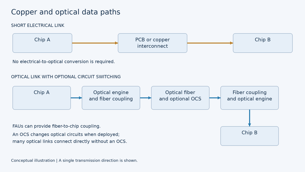
A short copper link stays electrical from end to end. It needs no optical engine, optical fiber or optical fiber array unit. In an optical link, the optical engine performs conversion, the fiber carries the light, and a fiber array may provide the precision connection to a photonic chip.
What an optical circuit switch does
A conventional electronic packet switch receives a signal, processes packet information and selects an output. When its ports are optical, transceivers convert between optical and electrical domains at those ports. Electrical packet switching remains valuable for flexible, fine-grained forwarding.
An optical circuit switch, or OCS, establishes physical optical paths between ports. The optical payload passes through without packet-by-packet electrical decoding inside the OCS. Its controller and actuators still use electrical power. Established circuits can reduce intermediate conversion and switching stages in a suitable network design.
Reconfiguration time must be distinguished from the transit delay of an already established circuit. MEMS-based OCS systems can switch on millisecond timescales, while other optical switching technologies have different characteristics. Traffic scheduling and topology control therefore matter as much as the optical hardware.
There is no universal 95 percent latency reduction, 50–90 percent power saving, or mandatory OCS-spine and electronic-leaf topology. Benefits depend on the baseline and architecture. Optical circuits and electronic packet switches are often complementary; the best mix depends on workload and operational requirements.
6 FAUs and the precision of fiber to chip coupling
A fiber array unit, or FAU, positions multiple optical fibers in a controlled arrangement so that they can couple efficiently to a photonic device. It is a passive optical assembly and is relevant to optical links rather than pure copper connections.
Depending on the design, an FAU may use precision grooves, a cover or substrate, adhesives, lenses, or other optical features. These are not a mandatory bill of materials for every FAU. Edge coupling and vertical coupling use different geometries, and the required alignment tolerance depends on the optical interface.
Why alignment matters
The optical field emerging from a fiber must overlap the intended field at the chip interface. Misalignment, angular error, gaps and mode mismatch raise coupling loss. Thermal expansion and mechanical movement can change that alignment after assembly.
For scale, some single-mode fibers have a core diameter around 9 micrometers, and some silicon waveguides have submicrometer cross-sections. These are illustrative dimensions, not universal specifications. The physical core diameter, mode field diameter and alignment tolerance are different quantities; one should not substitute for another.
LC and MPO connectors provide fiber-to-fiber connections elsewhere in a system. They do not by themselves perform the fine optical coupling between a fiber and a silicon waveguide. An FAU or another engineered coupling interface addresses that boundary.
Manufacturing and thermal integration
Higher channel counts make assembly yield, alignment speed, reliability and test access increasingly important. Optical attachment must be coordinated with the semiconductor packaging process. Whether fiber attachment occurs before or after reflow depends on the selected materials and process; it is not accurate to say that all optical fiber cannot tolerate reflow temperatures.
7 Detachable fiber arrays and serviceability
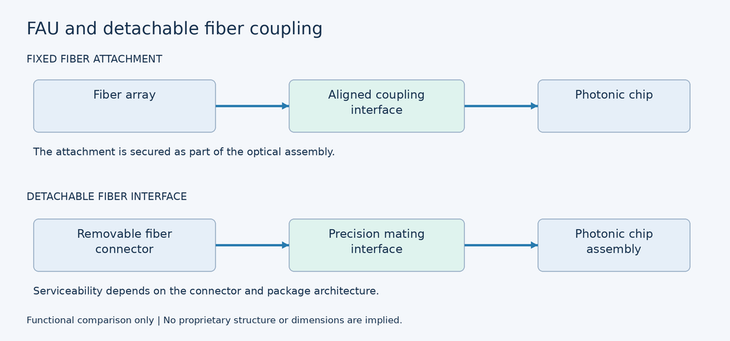
A permanently attached fiber array can complicate assembly and repair when an optical connection needs replacement. The consequences depend on the package design: a damaged fiber does not automatically require scrapping an entire ASIC board, and external laser modules may already be separately replaceable.
Detachable fiber interfaces separate a removable fiber connection from the chip-side assembly. Some suppliers describe these as detachable fiber array units, or DFAUs, although names and mechanical implementations differ. The goal is to combine low coupling loss with repeatable alignment and practical assembly or service procedures.
Potential advantages
Replace an accessible fiber connection without disturbing the core semiconductor assembly, where the architecture permits.
Separate selected optical attachment operations from semiconductor packaging steps.
Support modular assembly and testing while maintaining the required optical performance.
What engineers still need to validate
A detachable interface adds its own requirements: insertion loss, return loss, mating repeatability, contamination control, retention, thermal stability and supported mating cycles. Replaceability is useful only if the interface maintains the required optical budget and reliability over its intended life.
Development directions include higher fiber counts, denser arrays, alternative coupling geometries and more standardized interfaces. There is no general basis for assigning every DFAU a three-to-five-times price premium, or for predicting it will be the first CPO component market to expand. Those claims require product and market evidence.
Choosing the right electrical and optical boundaries
Copper and optics solve different parts of the same interconnect problem. Use copper where a qualified electrical channel meets the reach, bandwidth, power and cost requirements. Use optical links where the system benefits justify the conversion and packaging complexity. Rack boundaries alone do not determine that choice.
Optical engines perform conversion, fiber provides low-loss transport, and OCS can add reconfigurable optical paths where the architecture calls for them. FAUs and detachable interfaces address the precision and serviceability of fiber-to-chip coupling. Together, these technologies help systems scale toward higher aggregate bandwidth, including 800G, 1.6T and emerging 3.2T applications, without making every part of the link interchangeable.